
What is the purpose of the single point ground connection for Power Integrations switchers?
Hello,
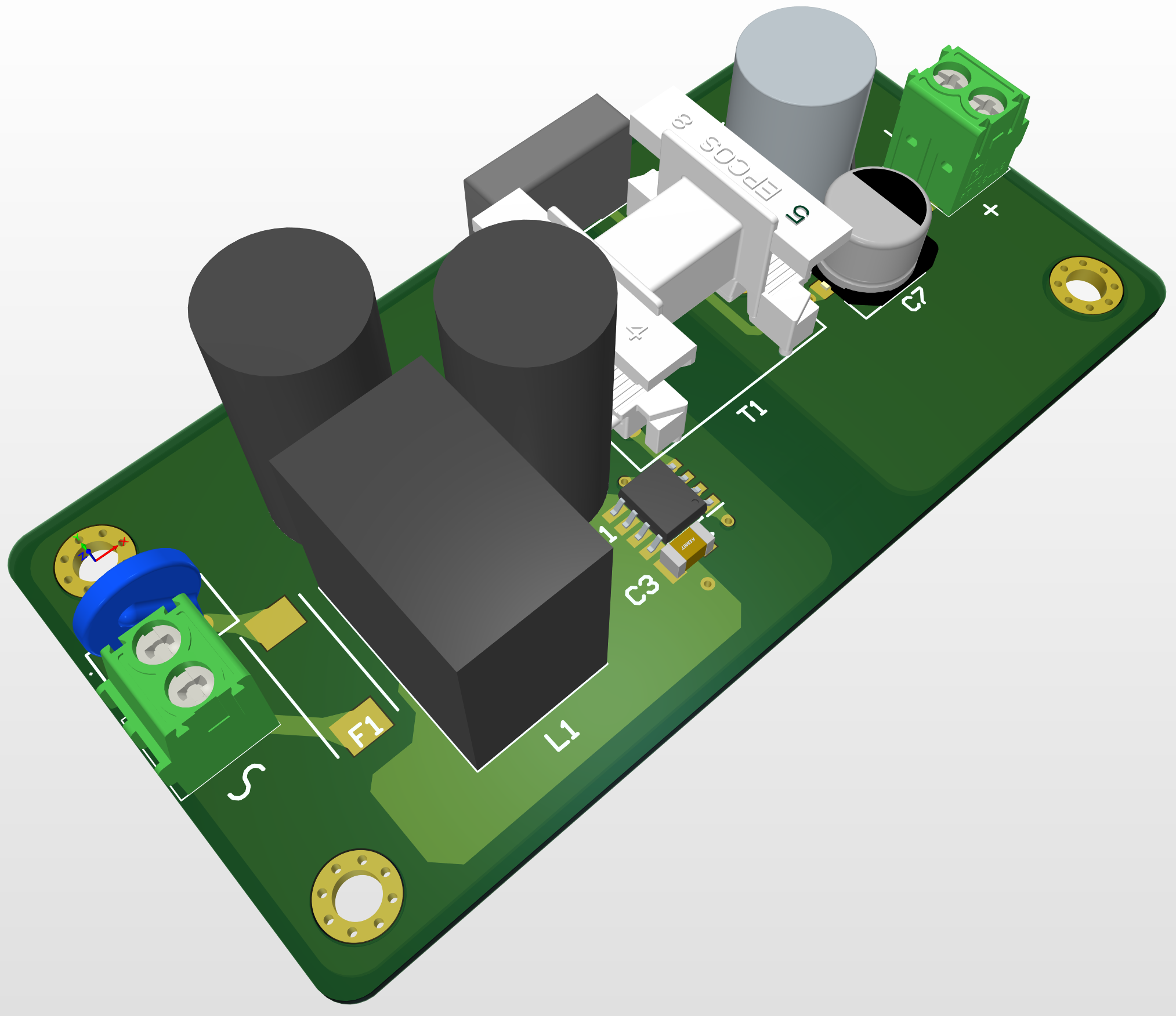
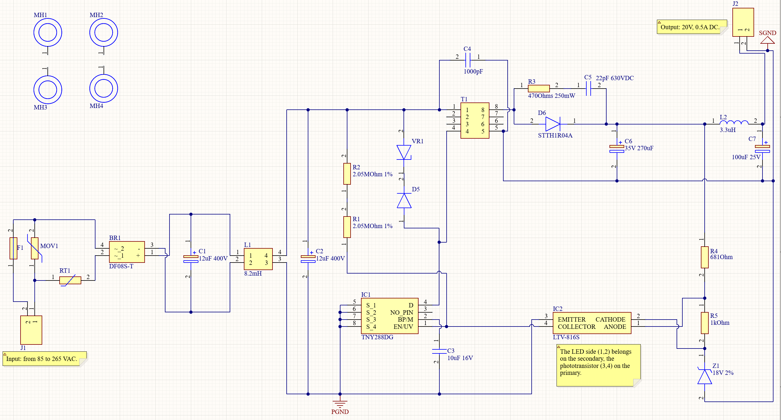
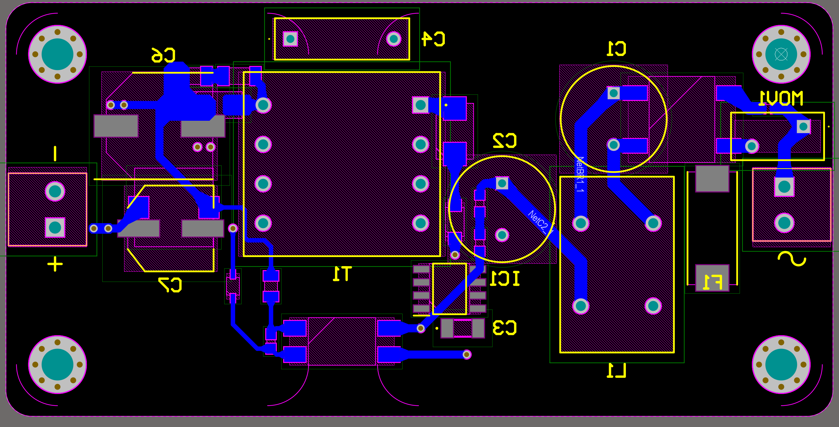
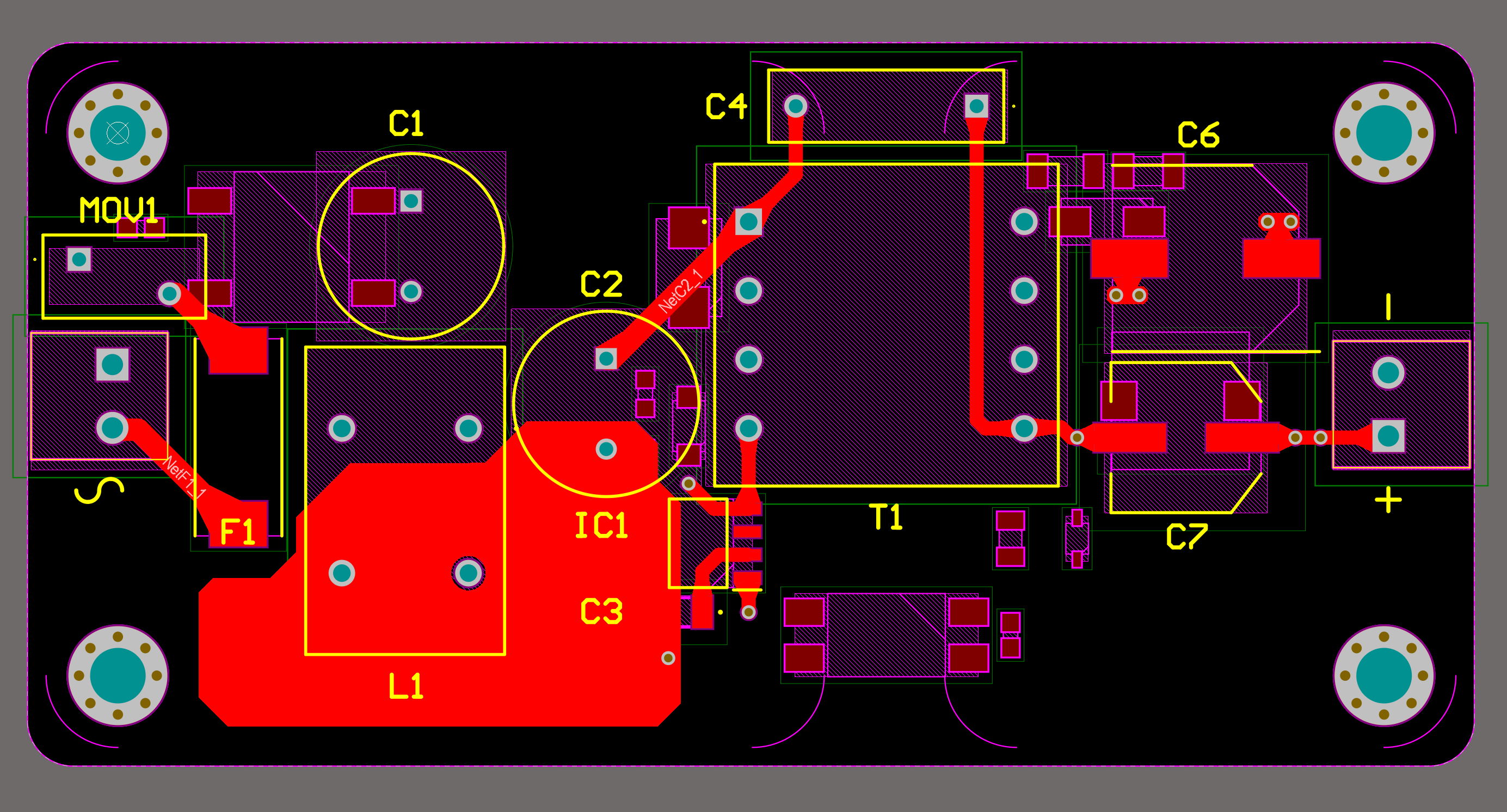
I am making a SMPS using TNY288DG (AC input ranging from 85 to 265VAC, DC output 20V, 0.5A). The circuits from PIExpert and from a designer program are in the attachments (they both are slightly different because sometimes I had to use other components than determined by PIExpert). The current PCB layout is also in the attachments.
I am using a four-layer board for the PCB. The layers are:
- Top (first) layer: Components and tracks.
- Second layer: Primary side and secondary side grounds.
- Third layer: Primary side and secondary side grounds.
- Bottom (fourth) layer: Components and Tracks.
In the recommendations in the TNY284-290 datasheet states the following: Use a single point ground connection from the input filter capacitor to the area of copper connected to the SOURCE pins. (Page 10).
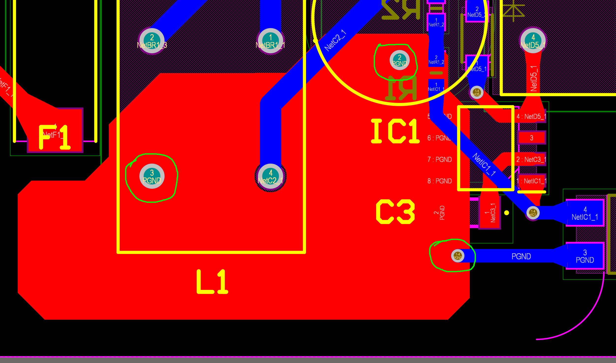
My questions are: Why should one use a single point ground connection, as specified in the datasheet? What is the reason for this? What happens if I deviate from this rule? As you can see in the attachment named "Shows where there is a connection to the primary ground (marked in green)", I have three ground connections: The polygon pour which is connected to the four source-pins of the switcher is connected to the primary ground at three points. Will it have negative effects?
If you're interested in why I use a four-layer board: I've heard from several prominent electrical engineers that a four-layer PCN is good for a SMPS, mainly for EMI reasons. However, for many (perhaps almost all) switchers from Power Integrations, there are examples of PCB layouts with only one or at most two layers. What is the reason for that? Does the use of a four-layer PCB in my case make the TNY288DG switcher less performant?
Thanks in advance!
Files
| Attachment | Size |
|---|---|
| 3D view of the board. | 527.71 KB |
| 3D view of the board (bottom side). | 390.3 KB |
| The schematic of the circuit in the Altium Designer. | 350.83 KB |
| Shows where there is a connection to the primary ground (marked in green). | 230.1 KB |
| Bottom layer of the PCB. | 353.04 KB |
| Top layer of the pcb. | 337.96 KB |
| The original schematic of the circuit from PIExpert. | 141.11 KB |
Comments
Hello Jedidiah,
thank you for your answer.
>I don't understand what you mean but page 11 in the datasheet shows layout example that can guide you....
In the attachment with the description "Shows where there is a connection to the primary ground (marked in green)." you see I have a polygon pour on the top layer of the PCB. This polygon pour is connected to all four source pins of TNY288DG. This polygon pour is also connected to the primary ground in three places:
- At the place with the negative pin of the bulk capacitor.
- At the place of a pin of the common mode choke.
- At the place where the track from pad no. 3 of the optocoupler.
All these connection points are marked in green in the attachment. Since there are three connection points, it is not a single-point ground connection anymore as stated in the datasheet, but three-point ground connection. Will this three-point ground connection have any negative impact on TNY288DG or maybe the whole board?
Additionally I would like to know if I can do the layout of the primary side of the SMPS without this polygon pour on the first layer.
Since I have a four layer PCB with two ground planes, I would make a much smaller polygon pour with four or more vias next to the source pins of TNY288DG. These vias would stitch this small polygon with the primary ground plane underneath together and they would also transfer the heat to the primary ground plane. I would also connect one pad of the bypass capacitor C3 with this polygon. I would make a via directly near the pad nr. 3 of the optocoupler which would stitch this pad with the primary ground plane underneath.
Best regards
Hi,
Single point connection means all the traces ended up connecting on one point regardless whether your connect 3, 4, 5 traces...on that point. Some engineering industry terminology call it star connection.
Regards,
Jedidiah
Would you delete the primary ground plane completely from my PCB and instead of this use this single-point ground connection rule?
I'm just trying to get some benefit from the four layer PCB. If I've deleted the ground plane, there's no point in using a four layer board for my PCB anymore. At least for the primary side of the PCB it won't make any sense.
Hi,
Of course not. Single point connection doesn't mean you can't use ground plane. Ground plane is always used in power supply design especially in helping reduced thermals in the switching MOSFET.
Attached here is the sample for your reference. L1 ground connection now goes directly to you Bulk Ground. From bulk ground connects your IC1 ground. In short, there are now single point connected to Bulk ground. I hope this helps....
Regards,
Jedidiah
| Attachment | Size |
|---|---|
| Layout sample.png | 330.66 KB |
Hello Jedidiah,
ok, you basically split the polygon but there's still a small connection next to the bulk capacitor pin. Do I understand correctly that by still being the same polygon, the heat is evenly distributed on it? So if I follow your advice I will have both a single point ground connection and a relatively large polygon for heat dissipation from the switcher?
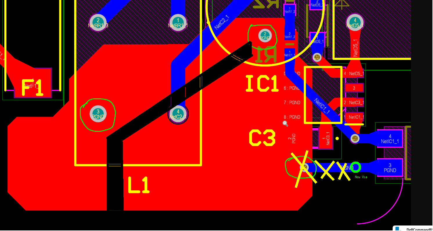
Another question. May I place the via that connects the pad 3 of the optocoupler to PGND right next to the pad of the optocoupler as shown in the attached picture (I painted the new via in green)? From my point of view there is nothing wrong with that.
Best Regards
| Attachment | Size |
|---|---|
| ScreenshotPCB_0.png | 250.92 KB |
Hi,
Yes, connecting with via should be fine.
Regards,
Jedidiah
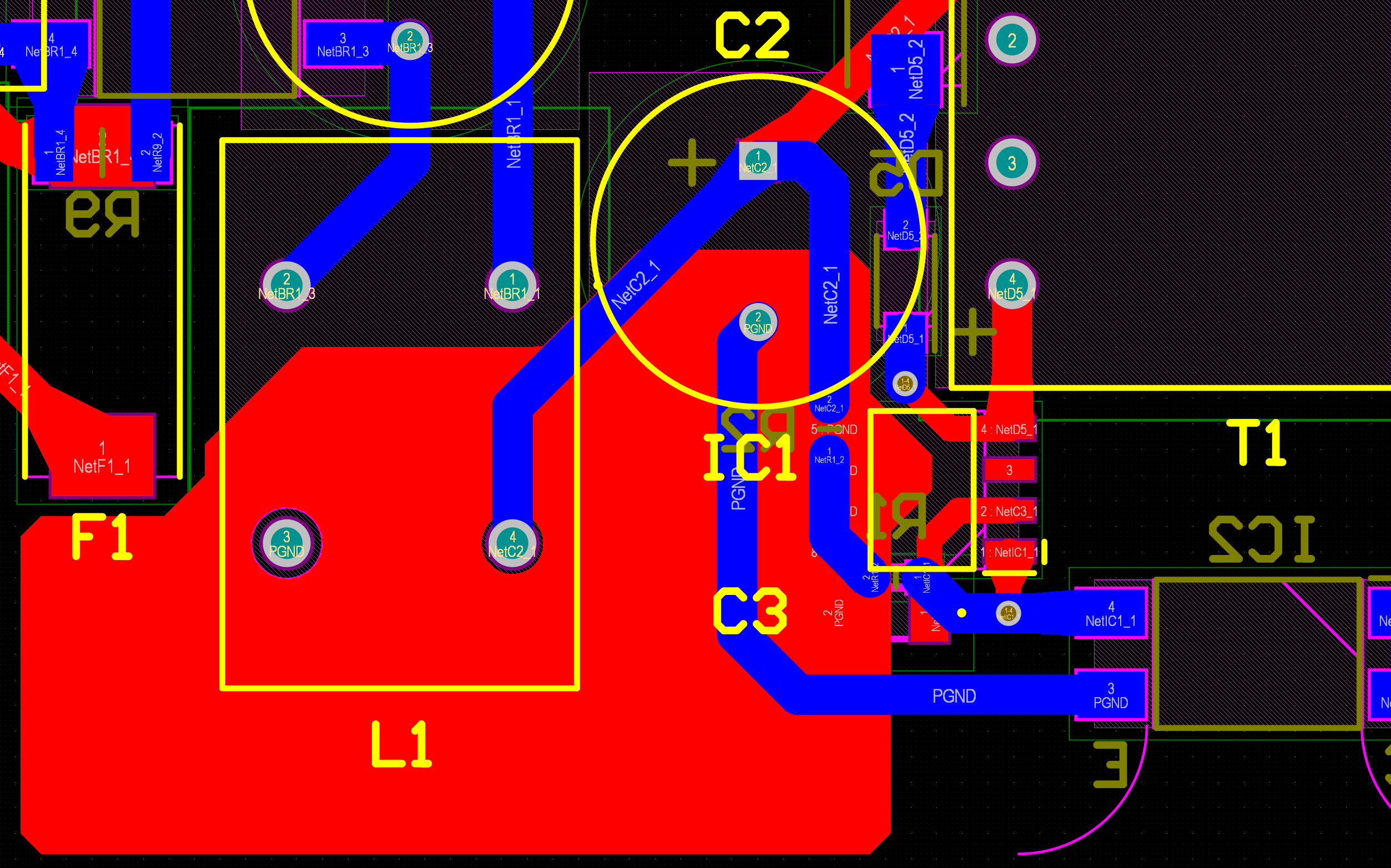
I had a discussion about the single-point ground connection on another forum. After that, I decided to connect the components in the following way (see attached picture). The polygon pour on the top layer is now connectet only to the minus pin of the bulk capacitor and to the SOURCE pin of the TNY286DG. On the bottom layer, the pad 3 of the optocoupler connected to the minus pin of the bulk capacitor with a track.
Question: Do you think the new connection from the picture is better than all privios variants?
Obviously I had trouble understanding what single-point ground connection means (although this is meant to be trivial). In my opinion I now actually have single point ground connection as recommended in the documentation. At least on the primary side.
| Attachment | Size |
|---|---|
| Polygon_with_TNY286DG_without_via.png | 347.24 KB |
It looks fine.
Regards,
Jedidiah
Hi CircuitDesigner,
Below are my answers to your questions:
Why should one use a single point ground connection, as specified in the datasheet? What is the reason for this?
--> Basically, if you other circuit like bias circuit that supplies BP/M like shown in page 11, it is always best to connect it to bulk capacitor grounding rather than the source pad of the IC so as any noise will not be seen on the source pin.
What happens if I deviate from this rule?
--> There are several testing required in a power supply such as ESD, surge, eft, etc.... The most stable ground node in a power supply is usually the power ground pin such as bulk capacitor. It is best to always use this node as your main ground reference so as to prevent any noise coupling towards the source pin of the IC.
The polygon pour which is connected to the four source-pins of the switcher is connected to the primary ground at three points. Will it have negative effects?
--> I don't understand what you mean but page 11 in the datasheet shows layout example that can guide you....
However, for many (perhaps almost all) switchers from Power Integrations, there are examples of PCB layouts with only one or at most two layers. What is the reason for that?
--> One layer PCB is the most cost effective way of designing power supply. Typically, in power 15W or less, it is not practical to use expensive multilayer boards.
Does the use of a four-layer PCB in my case make the TNY288DG switcher less performant?
--> No. More layer PCB is always better but more expensive.
Regards,
Jedidiah